The graphics card is one of the most complex hardware components in a computer. At first glance, it looks like just a metal block with fans and a chip, but inside it is a precisely controlled process of working with data. While VRAM (Video RAM) stores huge amounts of information for games, models or videos, its speed is not enough to supply thousands of parallel computing cores. That’s why the GPU uses an array of fast caches, registers and dedicated memory layers that together form the GPU internal memory – an important link between the core and the main VRAM.
In the previous article, we discussed VRAM itself – memory types such as GDDR, HBM or LPDDR. This time, however, we’ll look deeper – right into the GPU core, where it decides how fast the card can process data, render an image or compute thousands of parallel operations. And it’s the GPU internal memory that plays a major role here.
VRAM versus GPU internal memory – two worlds of one graphics
VRAM, the video memory of a graphics card, is external to the GPU chip itself. It stores large amounts of data – textures, models, frame buffers or shader programs. It is a fast memory, but due to the fact that it is located outside the core, it has a higher latency than the internal memory of the graphics card. Data is transferred over a memory bus (e.g., 256-bit or 384-bit, etc.) whose width and frequency determine throughput.
While modern memories like GDDR6X or GDDR7 achieve blazing speeds, the GPU would be inefficient if it had to constantly reach for data from VRAM. Therefore, smaller but much faster memories are built inside the chip to serve as an extended arm of the compute cores. Together, these components form the GPU internal memory, which acts as a smart intermediate between the core and VRAM.
How GPU memory architecture works
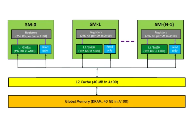
The memory architecture of a graphics card works like a perfectly organized factory where each element has a precise role. VRAM is a huge warehouse – it contains all the textures, data, instructions and models that the GPU needs for computations. Cache memories function as distribution racks that prepare data for immediate use, while registers are the actual “workers” that work directly with them. Together, they form a complex network in which information moves in well-defined cycles and speed levels.
Each GPU compute unit – whether it’s a streaming multiprocessor (SM) in NVIDIA’s architecture or a compute unit (CU) in AMD’s architecture – has its own L1 cache and registers. These units process hundreds to thousands of threads in parallel, with each thread needing immediate access to its data. To avoid slowdowns, the GPU constantly moves data between caches, registers and VRAM so that it is always in the right place at the right time. This process is managed by the memory controller, which decides when and where to transfer the information.
The goal of the entire architecture is to shorten the distance that information must travel. This is because accessing VRAM has an order of magnitude higher latency than internal on-chip memory. Therefore, the GPU stores the most important data as close as possible to the compute cores – in caches or registers. This minimizes latency and maximizes the number of operations the card can process in a single clock cycle.
A system designed in this way works in a continuous cycle: instruction → data fetch → calculation → result storage → cache update. Thanks to this, modern chips can process billions of instructions per second, with the smooth flow of information being handled by the GPU internal memory, which serves as a fast bridge between the core and the main VRAM.
Memory cache – the brain of the GPU memory architecture
The cache layers are the backbone of the system, represented by the GPU internal memory. These ensure that the compute cores have immediate access to the data they need most often. There are multiple levels of caches in a graphics chip, from smaller and faster ones to larger ones that serve as an intermediate layer between the core and VRAM. Their job is to keep data constantly moving so that the GPU doesn’t wait a single clock.
- L1 caches are found at compute blocks – for example, at shader units in AMD architectures or at streaming multiprocessors (SM) in NVIDIA chips. It stores a small amount of data that is being processed at any given time. The access time is extremely short – on the order of a few clock cycles.
- The L2 cache is larger and shared between multiple blocks. It serves as a central swap zone where the results of computations are stored and accessed by different parts of the GPU. Together with the lower cache levels, it forms the basis of the system, which is the GPU internal memory and ensures fast communication between the core and VRAM.
- Infinity Cache represents the highest level of cache in AMD architectures . It is not a classic L3 cache, but it functions similarly – as a large intermediate layer that increases the effective throughput of the memory system.
The 2025 RDNA 4 architecture uses a third-generation Infinity Cache with up to 64 MB of capacity (depending on model) and improved interconnect to the L2 cache, increasing effective throughput and reducing the burden on VRAM. NVIDIA follows the same principle – the Ada Lovelace generation offers up to 96 MB of L2 cache in the AD102 chip, while the newer Blackwell architecture expands it to up to 128 MB. In both cases, these are maximum capacities that may vary depending on the specific model, but the goal remains the same – to speed up the data flow between the kernel and the memory system and increase the efficiency provided by the GPU’s internal memory.
Registers and SRAM – speed directly in the GPU core
If caches are the brains of the graphics card, registers are its reflexes. They reside directly in the compute units and store the values that the GPU is currently working with – for example, data when calculating light, shadows or motion. Their instant response and high speed are among the main reasons why the GPU internal memory is able to process huge amounts of data without lag.
Each core has its own set of registers. The NVIDIA Ada Lovelace architecture has up to 65,536 of them per multiprocessor, and they are dynamically distributed among threads according to the computational needs. AMD RDNA 4 uses a similar principle, where registers are optimized for wave32 and wave64 instruction processing. Combined with cache layers, they ensure maximum computation speed and smooth operation of the entire GPU.
Special memory types within the GPU
In addition to the classic cache and register layers, some GPUs use special solutions. In mobile GPUs, such as the Apple A-series, ARM Mali or Qualcomm Adreno chips, the Tile-Based Deferred Rendering (TBDR) architecture is used. The GPU processes the image in smaller blocks – called tiles – which it stores in local tile memory. This approach significantly improves efficiency and contributes to the GPU internal memory being able to operate more efficiently and with lower power consumption.
In integrated graphics solutions such as AMD APUs, Intel Arc Xe, Iris Xe or Apple M-series, in turn, shared system memory is used. This is a shared space for both the CPU and the GPU that allows direct access to data without having to copy it. While this approach saves power and simplifies the architecture, it falls short of the performance offered by dedicated internal GPU memory.
Conclusion
Modern graphics cards have long since stopped building on VRAM capacity alone. Their real performance is also determined by the internal memory architecture, which determines both the processing speed and the overall efficiency of the chip, thanks to the solutions that the GPU internal memory combines. Developments are moving towards throughput optimization and intelligent data management, enabling today’s GPUs to achieve higher performance at lower power. It is this balance between speed, throughput and efficiency that will determine the direction that future generations of graphics cards will take.